《Electronics Lab》课程教学资源:Lab 05 & 06 op-amp:adder、Integrator & Differentiator
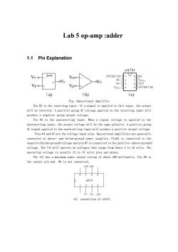
Lab 5 op-amp adder 1.1 Pin Explanation uA741 Vno- OFFSET N1 oVo Vo IN- Vcct Vp IN+ 3 OUT Vcc- OFFSET N2 (a) (b) (c) Fig.Operational Amplifier Pin #2 is the inverting input.If a signal is applied to this input,the output will be inverted.A positive going AC voltage applied to the inverting input will produce a negative going output voltage. Pin #3 is the noninverting input.When a signal voltage is applied to the noninverting input,the output voltage will be the same polarity.A positive going AC signal applied to the noninverting input will produce a positive output voltage. Pins #4 and #7 are the voltage input pins.Operational amplifiers are generally connected to above-and below-ground power supplies.Pin#4 is connected to the negative(below-ground)voltage and pin #7 is connected to the positive(above-ground) voltage.The 741 will operate on voltages that range from about 4 to 16 volts.The operating voltage is usually 12 to 15 volts plus and minus. The 741 has a maximum power output rating of about 500 milliwatts.Pin #6 is the output pin and #8 is not connected. +12V OUT uA741 234 Vi-Vi+-12V (a)connection of uA741
Lab 5 op-amp :adder 1.1 Pin Explanation Fig. Operational Amplifier Pin #2 is the inverting input. If a signal is applied to this input, the output will be inverted. A positive going AC voltage applied to the inverting input will produce a negative going output voltage. Pin #3 is the noninverting input. When a signal voltage is applied to the noninverting input, the output voltage will be the same polarity. A positive going AC signal applied to the noninverting input will produce a positive output voltage. Pins #4 and #7 are the voltage input pins. Operational amplifiers are generally connected to above- and below-ground power supplies. Pin#4 is connected to the negative(below-ground)voltage and pin #7 is connected to the positive (above-ground) voltage. The 741 will operate on voltages that range from about 4 to 16 volts. The operating voltage is usually 12 to 15 volts plus and minus. The 741 has a maximum power output rating of about 500 milliwatts. Pin #6 is the output pin and #8 is not connected. uA741 123 5 4 8 6 7 +12V Vi- Vi+ OUT -12V (a) connection of uA741
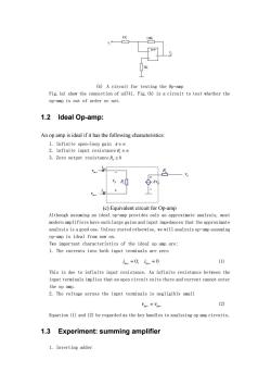
(b)A circuit for testing the Op-amp Fig.(a)show the connection of uA741.Fig.(b)is a circuit to test whether the op-amp is out of order or not. 1.2 Ideal Op-amp: An op amp is ideal if it has the following characteristics: 1.Infinite open-loop gain A=o 2.Infinite input resistance R,=o 3.Zero output resistance R,=0 (c)Equivalent circuit for Op-amp Although assuming an ideal op-amp provides only an approximate analysis,most modern amplifiers have such large gains and input impedances that the approximate analysis is a good one.Unless stated otherwise,we will analysis op-amp assuming op-amp is ideal from now on. Two important characteristics of the ideal op amp are: 1.The currents into both input terminals are zero in+=0,m-=0 (1) This is due to infinite input resistance.An infinite resistance between the input terminals implies that an open circuit exits there and current cannot enter the op amp. 2.The voltage across the input terminals is negligibly small Vint Vin- (2) Equation (1)and(2)be regarded as the key handles to analyzing op amp circuits. 1.3 Experiment:summing amplifier 1.Inverting adder
i v o v (b) A circuit for testing the Op-amp Fig.(a) show the connection of uA741. Fig.(b) is a circuit to test whether the op-amp is out of order or not. 1.2 Ideal Op-amp: An op amp is ideal if it has the following characteristics: 1. Infinite open-loop gain A 2. 1nfinite input resistance Ri 3. Zero output resistance 0 Ro Ri Ro A d d v v o v in v in v in i in i (c) Equivalent circuit for Op-amp Although assuming an ideal op-amp provides only an approximate analysis, most modern amplifiers have such large gains and input impedances that the approximate analysis is a good one. Unless stated otherwise, we will analysis op-amp assuming op-amp is ideal from now on. Two important characteristics of the ideal op amp are: l. The currents into both input terminals are zero 0; 0 in in i i (1) This is due to infinite input resistance. An infinite resistance between the input terminals implies that an open circuit exits there and current cannot enter the op amp. 2. The voltage across the input terminals is negligibly small in in v v (2) Equation (1) and (2) be regarded as the key handles to analyzing op amp circuits. 1.3 Experiment: summing amplifier 1. Inverting adder
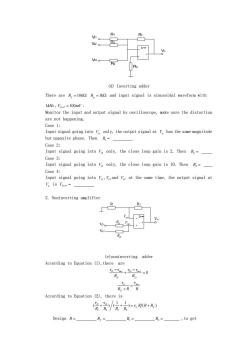
V1。 R1 R2 (d)Inverting adder There are R,=10kQ R,=Ik and input signal is sinusoidal waveform with IkH=,Vp-p =100mV. Monitor the input and output signal by oscilloscope,make sure the distortion are not happening. Case 1: Input signal going into V only,the output signal at V has the same magnitude but opposite phase.Then R= Case 2: Input signal going into v only,the close loop gain is 2.Then R= Case 3: Input signal going into V:only,the close loop gain is 10.Then R= Case 4: Input signal going into Va,V2 and Vs at the same time,the output signal at V。is'n-p= 2.Noninverting amplifier R Rr Vilo Vi2 (e)noninverting adder According to Equation (1),there are Ya-Ya:+Y2-Vat=0 R R R+RR According to Equation (2),there is /11 色+2) 十 )='。R/R+Rr) Design R=_ R=_ R=. R= to get
(d) Inverting adder There are 10 R k f 1 R k p and input signal is sinusoidal waveform with 1kHz , 100 V mV P P . Monitor the input and output signal by oscilloscope, make sure the distortion are not happening. Case 1: Input signal going into Vi1 only, the output signal at Vo has the same magnitude but opposite phase. Then R1 Case 2: Input signal going into Vi2 only, the close loop gain is 2. Then R2 Case 3: Input signal going into Vi3 only, the close loop gain is 10. Then R3 Case 4: Input signal going into Vi1 ,Vi2 and Vi3 at the same time, the output signal at Vo is VP P 2. Noninverting amplifier Ri1 Vin Ri2 Vin (e)noninverting adder According to Equation (1),there are 1 2 1 2 0 i in i in i i vv vv R R o in f v v RR R According to Equation (2), there is 1 2 12 12 1 1 ( )( ) ( ) i i o f v v vR R R RR RR Design R Rf R1 R2 ,to get
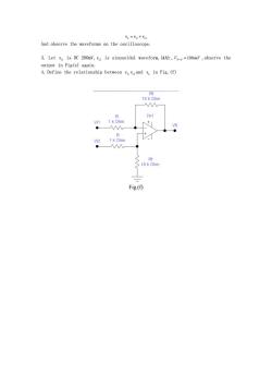
V。='a+'2 And observe the waveforms on the oscilloscope. 3.Let va is DC 200mV,v2 is sinusoidal waveform,k,V_p=100ml,observe the output in Fig(e)again. 4.Define the relationship between va v and v in Fig.(f) Rf 10 k Ohm R 741 Vi1 1 k Ohm vo R Vi2 1 k Ohm 10 k ohm Rf Fig.(f)
oi i 1 2 vvv And observe the waveforms on the oscilloscope. 3. Let i1 v is DC 200mV, i2 v is sinusoidal waveform,1kHz , 100 V mV P P ,observe the output in Fig(e) again. 4. Define the relationship between i1 v i2 v and o v in Fig.(f) Fig.(f)

Lab 6 Integrator Differentiator 2.1 Integrating circuit K 300KQ C10.1uF 30KQ Ri Uo 30KQ Rp Fig.(a)Integrating circuit 1.input signal IkH,V_p=IV,Square waveform. Observe the input and output signals at the same time.Measure the magnitudes both with cursors by oscilloscope. Input magnitude: Output magnitude:
Lab 6 Integrator & Differentiator 2.1 Integrating circuit Fig.(a) Integrating circuit 1.input signal : 1kHz , 1 V V P P ,Square waveform. Observe the input and output signals at the same time. Measure the magnitudes both with cursors by oscilloscope. Input magnitude: Output magnitude:

2.input signal 2kH,V_=IV,Square waveform. Input magnitude: Output magnitude: 3.input signal 500H,Vp=IV,Square waveform. Input magnitude: Output magnitude: 4.input signal IkH,V_p=2V,Square waveform. Input magnitude: Output magnitude: 5.input signal Ik,Vp=500mV,Square waveform. Input magnitude: Output magnitude:
2.input signal : 2kHz , 1 V V P P ,Square waveform. Input magnitude: Output magnitude: 3.input signal : 500Hz , 1 V V P P ,Square waveform. Input magnitude: Output magnitude: 4.input signal : 1kHz , 2 V V P P ,Square waveform. Input magnitude: Output magnitude: 5. input signal : 1kHz , 500 V mV P P ,Square waveform. Input magnitude: Output magnitude:

2.2 Differentiators circuit 30K RI C1 30000.1μF 3002 Fig.(b)Differentiators circuit input signal Ikz,Vp=60mV,Square waveform. Observe the input and output signals at the same time.Measure the magnitudes both by cursors with oscilloscope. Input magnitude: Output magnitude:
2.2 Differentiators circuit Fig.(b) Differentiators circuit input signal : 1kHz , 60 V mV P P ,Square waveform. Observe the input and output signals at the same time. Measure the magnitudes both by cursors with oscilloscope. Input magnitude: Output magnitude:
按次数下载不扣除下载券;
注册用户24小时内重复下载只扣除一次;
顺序:VIP每日次数-->可用次数-->下载券;
- 《Electronics Lab》课程教学资源:Lab 04 counters.pdf
- 《Electronics Lab》课程教学资源:Lab 03 Edged-triggered Flip-Flops.pdf
- 《Electronics Lab》课程教学资源:Lab 02 Decoder and demultiplexer.pdf
- 《Electronics Lab》课程教学资源:Lab 12&13 Feedback amplifiers.pdf
- 《Electronics Lab》课程教学资源:Lab 11 OBJECTIVES.pdf
- 《Electronics Lab》课程教学资源:Lab 01 Combinational Logic.pdf
- 上海交通大学:《微电子学概论》课程教学资源_图灵奖下的人类智力延伸——-计算、集成电路及应用.pdf
- 《微电子学概论》课程教学资源:用十分鐘瞭解《圖靈獎得主》的學術貢獻.pdf
- 《数字集成电路 Digital Integrated Circuit》课程教学资源(阅读资料)IC testing_Novel Applications of Deep Learning Hidden Features for Adaptive Testing.pdf
- 《数字集成电路 Digital Integrated Circuit》课程教学资源(阅读资料)IC testing_IC design-for-test and testability features.pdf
- 《数字集成电路 Digital Integrated Circuit》课程教学资源(阅读资料)IC testing_Design, Manufacturing & Test of Integrated Circuits in the Nanotechnology Era.pdf
- 《数字集成电路 Digital Integrated Circuit》课程教学资源(阅读资料)IC testing_DESIGN AND TESTING OF COMBINATIONAL LOGIC CIRCUITS USING BUILT IN SELF TEST SCHEME FOR FPGAs.pdf
- 《数字集成电路 Digital Integrated Circuit》课程教学资源(阅读资料)IC testing_An introduction to IC testing.pdf
- 《数字集成电路 Digital Integrated Circuit》课程教学资源(阅读资料)IC testing_3D DFT challenges and solutions.pdf
- 上海交通大学:《数字集成电路 Digital Integrated Circuit》课程教学资源(课程实验)Lab #1:HSPICE Simulation.pdf
- 上海交通大学:《数字集成电路 Digital Integrated Circuit》课程教学资源(课程实验)HSPICE SIMULATION.pdf
- 上海交通大学:《数字集成电路 Digital Integrated Circuit》课程教学资源(讲义)Introduction(Semiconductor processing).pdf
- 上海交通大学:《电路基础》课程教学资源(PPT课件)第二章 电路分析的基本方法 §2.8 回路分析法 §2.9 节点分析法.ppt
- 上海交通大学:《通信基本电路》课程教学资源(参考资料)Fundamental of Communication Circuits Lecture 1 Introduction.ppt
- 上海交通大学:《电路基础》课程教学资源(PPT课件)第三章 电路定理 §3.4 互易定理.ppt
- 《Electronics Lab》课程教学资源:Lab 07 & 08 filter、Function Generator.pdf
- 《Electronics Lab》课程教学资源:Lab 09 & 10 Transistor Amplifier.pdf
- 上海交通大学:《通信原理与实验 Principles and Experiments of Communications》课程教学资源(PPT讲稿)Intro.ppt
- 《通信原理与实验 Principles and Experiments of Communications》课程参考书:John G. Proakis Masoud Salehi《Fundamentals of Communication Systems》(Second Edition).pdf
- 《Measurement Systems:Application and Design》课程教学资源(扩展知识)A Brief History of Measurement Systems.pdf
- 《Measurement Systems:Application and Design》课程教学资源(扩展知识)Cross-Linked Gold Nanoparticles on Polyethylene:Resistive Responses to Tensile Strain and Vapors.pdf
- 上海交通大学:《Measurement Systems:Application and Design》课程教学资源(扩展知识)Strain rate-dependent tensile properties and dynamic electromechanical response of carbon nanotube fibers.pdf
- 上海交通大学:《Measurement Systems:Application and Design》课程教学资源(扩展知识)In the memorial of a great author.pdf
- 上海交通大学:《Measurement Systems:Application and Design》课程教学资源(课件讲稿)Chapter 01 Introduction.pdf
- 上海交通大学:《Measurement Systems:Application and Design》课程教学资源(课件讲稿)Chapter 02 Configuration and Functional Description.pdf
- 上海交通大学:《Measurement Systems:Application and Design》课程教学资源(课件讲稿)Chapter 03 Generalized performance characteristics of instruments.pdf
- 上海交通大学:《Measurement Systems:Application and Design》课程教学资源(课件讲稿)Chapter 04 Motion & Dimensional Measurement.pdf
- 上海交通大学:《Measurement Systems:Application and Design》课程教学资源(课件讲稿)Chapter 05 Force Torque and Shaft Power Measurement.pdf
- 上海交通大学:《Measurement Systems:Application and Design》课程教学资源(课件讲稿)Chapter 06 Pressure and Sound Measurement.pdf
- 上海交通大学:《Measurement Systems:Application and Design》课程教学资源(课件讲稿)Chapter 07 Flow Measurement.pdf
- 上海交通大学:《Measurement Systems:Application and Design》课程教学资源(课件讲稿)Chapter 08 Temperature and Heat-Flux Measurement.pdf
- 上海交通大学:《Measurement Systems:Application and Design》课程教学资源(课件讲稿)Chapter 09 Miscellaneous Measurements.pdf
- 上海交通大学:《Measurement Systems:Application and Design》课程教学资源(课件讲稿)Chapter 10 Manipulating Computing and Compensation Devices.pdf
- 上海交通大学:《Measurement Systems:Application and Design》课程教学资源(课件讲稿)Chapter 11 Data Transmission and Instrument Connectivity.pdf
- 西安电子科技大学:《电路分析基础》精品课程电子教案(PPT课件讲稿)第1章 电路的基本概念与定律.ppt
