《电力电子技术》课程实验指导(参考资料)IRFP450
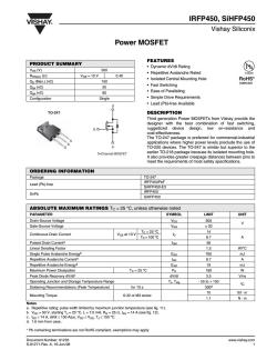
VISHAY. IRFP450,SiHFP450 Vishay Siliconix Power MOSFET FEATURES PRODUCT SUMMARY ·Dynamic dV/dt Rating Vos (V) 500 Ves=10V Repetitive Avalanche Rated RDsion)() 0.40 Qg(Max.)(nC) 150 Isolated Central Mounting Hole RoHS* Qgs(nC) 20 ·Fast Switching COMPLIANT Qgd(nC) 80 ·Ease of Paralleling Configuration Single Simple Drive Requirements 0 Lead(Pb)-free Available ● T0-247 DESCRIPTION Third generation Power MOSFETs from Vishay provide the designer with the best combination of fast switching, ruggedized device design,low on-resistance and cost-effectiveness. The TO-247 package is preferred for commercial-industrial applications where higher power levels preclude the use of TO-220 devices.The TO-247 is similar but superior to the N-Channel MOSFET earlier TO-218 package because its isolated mounting hole It also provides greater creepage distances between pins to meet the requirements of most safety specifications. ORDERING INFORMATION Package T0-247 IRFP450PbF Lead(Pb)-free SiHFP450-E3 SnPb IRFP450 SiHFP450 ABSOLUTE MAXIMUM RATINGS Tc =25C,unless otherwise noted PARAMETER SYMBOL LIMIT UNIT Drain-Source Voltage Vos 500 Gate-Source Voltage Vas ±20 Continuous Drain Current VGs at 10V Tc=25℃ 14 Tc=100C p 8.7 Pulsed Drain Currenta IDM 56 Linear Derating Factor 1.5 W/C Single Pulse Avalanche Energyb EAS 760 mJ Repetitive Avalanche Currenta IAR 8.7 A Repetitive Avalanche Energya EAR 19 mJ Maximum Power Dissipation Tc=25℃ Po 190 W Peak Diode Recovery dV/dte dV/dt 3.5 V/ns Operating Junction and Storage Temperature Range TJ,Tstg -55to+150 300d ℃ Soldering Recommendations(Peak Temperature) for 10s 10 Ibf.in Mounting Torque 6-32 or M3 screw 1.1 N.m Notes a.Repetitive rating;pulse width limited by maximum junction temperature (see fig.11). b.Vpp=50 V,starting TJ=25C,L=7.0 mH,RG =25 2,IAS=14 A (see fig.12). c.lso≤14A,dWt≤130AWμs,Vop≤Vos,Ty≤150C. d.1.6 mm from case. Pb containing terminations are not RoHS compliant,exemptions may apply Document Number:91233 www.vishay.com S-81271-Rev.A.16-Jun-08 1
Document Number: 91233 www.vishay.com S-81271-Rev. A, 16-Jun-08 1 Power MOSFET IRFP450, SiHFP450 Vishay Siliconix FEATURES • Dynamic dV/dt Rating • Repetitive Avalanche Rated • Isolated Central Mounting Hole • Fast Switching • Ease of Paralleling • Simple Drive Requirements • Lead (Pb)-free Available DESCRIPTION Third generation Power MOSFETs from Vishay provide the designer with the best combination of fast switching, ruggedized device design, low on-resistance and cost-effectiveness. The TO-247 package is preferred for commercial-industrial applications where higher power levels preclude the use of TO-220 devices. The TO-247 is similar but superior to the earlier TO-218 package because its isolated mounting hole. It also provides greater creepage distances between pins to meet the requirements of most safety specifications. Notes a. Repetitive rating; pulse width limited by maximum junction temperature (see fig. 11). b. VDD = 50 V, starting TJ = 25 °C, L = 7.0 mH, RG = 25 Ω, IAS = 14 A (see fig. 12). c. ISD ≤ 14 A, dI/dt ≤ 130 A/µs, VDD ≤ VDS, TJ ≤ 150 °C. d. 1.6 mm from case. PRODUCT SUMMARY VDS (V) 500 RDS(on) (Ω) VGS = 10 V 0.40 Qg (Max.) (nC) 150 Qgs (nC) 20 Qgd (nC) 80 Configuration Single N-Channel MOSFET G D S TO-247 G D S Available RoHS* COMPLIANT ORDERING INFORMATION Package TO-247 Lead (Pb)-free IRFP450PbF SiHFP450-E3 SnPb IRFP450 SiHFP450 ABSOLUTE MAXIMUM RATINGS TC = 25 °C, unless otherwise noted PARAMETER SYMBOL LIMIT UNIT Drain-Source Voltage VDS 500 V Gate-Source Voltage VGS ± 20 Continuous Drain Current VGS at 10 V TC = 25 °C ID 14 TC = 100 °C 8.7 A Pulsed Drain Currenta IDM 56 Linear Derating Factor 1.5 W/°C Single Pulse Avalanche Energyb EAS 760 mJ Repetitive Avalanche Currenta IAR 8.7 A Repetitive Avalanche Energya EAR 19 mJ Maximum Power Dissipation TC = 25 °C PD 190 W Peak Diode Recovery dV/dtc dV/dt 3.5 V/ns Operating Junction and Storage Temperature Range TJ, Tstg - 55 to + 150 °C Soldering Recommendations (Peak Temperature) for 10 s 300d Mounting Torque 6-32 or M3 screw 10 lbf · in 1.1 N · m * Pb containing terminations are not RoHS compliant, exemptions may apply
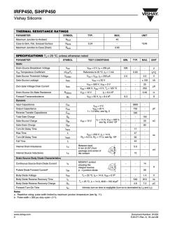
IRFP450,SiHFP450 VISHAY Vishay Siliconix THERMAL RESISTANCE RATINGS PARAMETER SYMBOL TYP. MAX. UNIT Maximum Junction-to-Ambient RthJA 40 Case-to-Sink,Flat,Greased Surface Rthcs 0.24 C/W Maximum Junction-to-Case (Drain) RthJc 0.65 SPECIFICATIONS TJ=25C,unless otherwise noted PARAMETER SYMBOL TEST CONDITIONS MIN. TYP.MAX.UNIT Static Drain-Source Breakdown Voltage Vos VGs=0V,lD=250μA 500 - V Vps Temperature Coefficient △Vps/Tj Reference to 25C,lp=1 mA 0.63 、 VC Gate-Source Threshold Voltage VGs(th) VDs VGS,Ip=250 HA 2.0 4.0 V Gate-Source Leakage lGss VGs=±20V ±100 nA Vos =500 V,Vas =0V 25 Zero Gate Voltage Drain Current Ioss μA VDs=400 V,Ves=0 V,TJ=125C 、 250 Drain-Source On-State Resistance Rps(on) VGs =10 V Ip =8.4 Ab 0.40 Forward Transconductance 9ts VDs=50 V,lo=8.4 A5 9.3 Dynamic Input Capacitance Ciss Ves=0V, 2600 Output Capacitance Coss Vos =25 V, 720 pF Reverse Transfer Capacitance Crss f=1.0 MHz,see fig.5 340 Total Gate Charge Qg 150 Gate-Source Charge Qgs VGs=10V ID =14 A,VDs =400 V, see fig.6 and 13b 20 nC Gate-Drain Charge Qgd 80 Turn-On Delay Time tdlon) 17 、 Rise Time t VDD =250 V,Ip=14 A, 47 ns Turn-Off Delay Time td(off) RG 6.2 Q,Ro=17Q,see fig.10b 92 Fall Time 44 Internal Drain Inductance Lo Between lead, 5.0 6 mm (0.25")from package and center of nH nternal Source Inductance Ls die contact 13 Drain-Source Body Diode Characteristics Continuous Source-Drain Diode Current g MOSFET symbol 14 showing the integral reverse Pulsed Diode Forward Currenta IsM p-n junction diode 56 Body Diode Voltage Vsp TJ=25℃,ls=14A,VGs=0V 1.4 V Body Diode Reverse Recovery Time tm 540 810 ns TJ-25℃,lF-14Ad/dt=100A/μsb Body Diode Reverse Recovery Charge Qrt 4.8 7.2μC Forward Turn-On Time ton Intrinsic turn-on time is negligible(turn-on is dominated by Ls and Lp) Notes a.Repetitive rating;pulse width limited by maximum junction temperature(see fig.11). b.Pulse width≤300us;duty cycle≤2%. www.vishay.com Document Number:91233 S-81271-Rev.A,16-Jun-08
www.vishay.com Document Number: 91233 2 S-81271-Rev. A, 16-Jun-08 IRFP450, SiHFP450 Vishay Siliconix Notes a. Repetitive rating; pulse width limited by maximum junction temperature (see fig. 11). b. Pulse width ≤ 300 µs; duty cycle ≤ 2 %. THERMAL RESISTANCE RATINGS PARAMETER SYMBOL TYP. MAX. UNIT Maximum Junction-to-Ambient RthJA - 40 Case-to-Sink, Flat, Greased Surface RthCS 0.24 - °C/W Maximum Junction-to-Case (Drain) RthJC - 0.65 SPECIFICATIONS TJ = 25 °C, unless otherwise noted PARAMETER SYMBOL TEST CONDITIONS MIN. TYP. MAX. UNIT Static Drain-Source Breakdown Voltage VDS VGS = 0 V, ID = 250 µA 500 - - V VDS Temperature Coefficient ΔVDS/TJ Reference to 25 °C, ID = 1 mA - 0.63 - V/°C Gate-Source Threshold Voltage VGS(th) VDS = VGS, ID = 250 µA 2.0 - 4.0 V Gate-Source Leakage IGSS VGS = ± 20 V - - ± 100 nA Zero Gate Voltage Drain Current IDSS VDS = 500 V, VGS = 0 V - - 25 µA VDS = 400 V, VGS = 0 V, TJ = 125 °C - - 250 Drain-Source On-State Resistance RDS(on) VGS = 10 V ID = 8.4 Ab - - 0.40 Ω Forward Transconductance gfs VDS = 50 V, ID = 8.4 Ab 9.3 - - S Dynamic Input Capacitance Ciss VGS = 0 V, VDS = 25 V, f = 1.0 MHz, see fig. 5 - 2600 - Output Capacitance Coss - 720 - pF Reverse Transfer Capacitance Crss - 340 - Total Gate Charge Qg VGS = 10 V ID = 14 A, VDS = 400 V, see fig. 6 and 13b - - 150 Gate-Source Charge Qgs - - 20 nC Gate-Drain Charge Qgd - - 80 Turn-On Delay Time td(on) VDD = 250 V, ID = 14 A, RG = 6.2 Ω, RD = 17 Ω, see fig. 10b - 17 - ns Rise Time tr - 47 - Turn-Off Delay Time td(off) - 92 - Fall Time tf - 44 - Internal Drain Inductance LD Between lead, 6 mm (0.25") from package and center of die contact - 5.0 - nH Internal Source Inductance LS - 13 - Drain-Source Body Diode Characteristics Continuous Source-Drain Diode Current IS MOSFET symbol showing the integral reverse p - n junction diode - - 14 A Pulsed Diode Forward Currenta ISM - - 56 Body Diode Voltage VSD TJ = 25 °C, IS = 14 A, VGS = 0 Vb - - 1.4 V Body Diode Reverse Recovery Time trr TJ = 25 °C, IF = 14 A, dI/dt = 100 A/µsb - 540 810 ns Body Diode Reverse Recovery Charge Qrr - 4.8 7.2 µC Forward Turn-On Time ton Intrinsic turn-on time is negligible (turn-on is dominated by LS and LD) D S G S D G
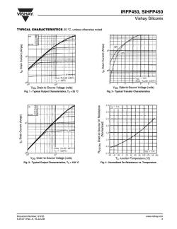
VISHAY. IRFP450,SiHFP450 Vishay Siliconix TYPICAL CHARACTERISTICS 25C,unless otherwise noted 1500 0 6 4.5- 20us PULSE WIDTH 「c=250c -20us PULSE WIDTH 10 09 101 8 0 Vps,Drain-to-Source Voltage (volts) VGs,Gate-to-Source Voltage (volts) Fig.1-Typical Output Characteristics,Tc =25C Fig.3-Typical Transfer Characteristics 3.5 0=14a 3.0 2.5 2.0 1,5 1.0 0.5 20Us PULSE WIDTH Tc■1500C 0 VGS 10V 100 101 0.0 60-40-20020406060100120140160 Vps,Drain-to-Source Voltage (volts) TJ,Junction Temperature(C) Fig.2-Typical Output Characteristics,Tc=150C Fig.4-Normalized On-Resistance vs.Temperature Document Number:91233 www.vishay.com S-81271-Rev.A.16-Jun-08 3
Document Number: 91233 www.vishay.com S-81271-Rev. A, 16-Jun-08 3 IRFP450, SiHFP450 Vishay Siliconix TYPICAL CHARACTERISTICS 25 °C, unless otherwise noted Fig. 1 - Typical Output Characteristics, TC = 25 °C Fig. 2 - Typical Output Characteristics, TC = 150 °C Fig. 3 - Typical Transfer Characteristics Fig. 4 - Normalized On-Resistance vs. Temperature

IRFP450,SiHFP450 VISHAY Vishay Siliconix VGS OV,T 1MHZ 0155= Cas SHOATED 5000 Crss O 400 C15 300 200 Co5 250g P55 1000 岛 VGS OV 12 1. 2.0 Vps,Drain-to-Source Voltage (volts) Vsp,Source-to-Drain Voltage (volts) Fig.5-Typical Capacitance vs.Drain-to-Source Voltage Fig.7-Typical Source-Drain Diode Forward Voltage 8 103 1D.14a Cs400 CPERATION IN THIS AREA LIMITED c52507 BY ROs (ON) 5:100 10 10 c=25°6 FOR TEST CIRCUIT T.=1500C SEE FIGURE 13 SINGLE PULSE 20 40 90100120 140 0.1 2 510 2 5 10225. 10 QG,Total Gate Charge (nC) Vps,Drain-to-Source Voltage (volts) Fig.6-Typical Gate Charge vs.Gate-to-Source Voltage Fig.8-Maximum Safe Operating Area www.vishay.com Document Number:91233 S-81271-Rev.A,16-Jun-08
www.vishay.com Document Number: 91233 4 S-81271-Rev. A, 16-Jun-08 IRFP450, SiHFP450 Vishay Siliconix Fig. 5 - Typical Capacitance vs. Drain-to-Source Voltage Fig. 6 - Typical Gate Charge vs. Gate-to-Source Voltage Fig. 7 - Typical Source-Drain Diode Forward Voltage Fig. 8 - Maximum Safe Operating Area
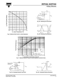
VISHAY. IRFP450,SiHFP450 Vishay Siliconix Rp Vos> D.U.T. R 几1ov Pulse widths 1 us Duty factor s0.1% Fig.10a-Switching Time Test Circuit 6 Vos 90% 25 50 75 400 125 150 10% Tc,Case Temperature(C) td(alf)4 Fig.9-Maximum Drain Current vs.Case Temperature Fig.10b-Switching Time Waveforms 0.1 SINGLE PULSE NOTES: -1.DUTY FACTOR,D-t1/t2 2.PEAK T;-PDM x Zthjc Tc o 105 10 10▣ 102 0.1 10 t1,Rectangular Pulse Duration (seconds) Fig.11-Maximum Effective Transient Thermal Impedance,Junction-to-Case Vary to obtain Vos required IAs Ra D.U.T 4 AS 10V 0.012 Fig.12a-Unclamped Inductive Test Circuit Fig.12b-Unclamped Inductive Waveforms Document Number:91233 www.vishay.com S-81271-Rev.A.16-Jun-08 5
Document Number: 91233 www.vishay.com S-81271-Rev. A, 16-Jun-08 5 IRFP450, SiHFP450 Vishay Siliconix Fig. 9 - Maximum Drain Current vs. Case Temperature Fig. 10a - Switching Time Test Circuit Fig. 10b - Switching Time Waveforms Fig. 11 - Maximum Effective Transient Thermal Impedance, Junction-to-Case Fig. 12a - Unclamped Inductive Test Circuit Fig. 12b - Unclamped Inductive Waveforms Pulse width ≤ 1 µs Duty factor ≤ 0.1 % RD VGS RG D.U.T. 10 V + - VDS VDD VDS 90 % 10 % VGS t d(on) t r t d(off) t f RG IAS tp 0.01 Ω D.U.T L VDS + - VDD A 10 V Vary tp to obtain required IAS IAS VDS VDD VDS tp
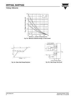
IRFP450,SiHFP450 VISHAY Vishay Siliconix 160 8.9A 14a 1200 B00 asind elbuls 恩 VoD 50V 必 50 75 100125150 Starting TJ.Junction Temperature(C) Fig.12c-Maximum Avalanche Energy vs.Drain Current Current regulator Same type as D.U.T. 10V -H- D.U.T. Vos NG 3mAE几 Charge- G Current sampling resistors Fig.13a-Basic Gate Charge Waveform Fig.13b-Gate Charge Test Circuit www.vishay.com Document Number:91233 6 S-81271-Rev.A,16-Jun-08
www.vishay.com Document Number: 91233 6 S-81271-Rev. A, 16-Jun-08 IRFP450, SiHFP450 Vishay Siliconix Fig. 12c - Maximum Avalanche Energy vs. Drain Current Fig. 13a - Basic Gate Charge Waveform Fig. 13b - Gate Charge Test Circuit QGS QGD QG VG Charge 10 V D.U.T. 3 mA VGS VDS I G I D 0.3 µF 0.2 µF 50 kΩ 12 V Current regulator Current sampling resistors Same type as D.U.T. + -
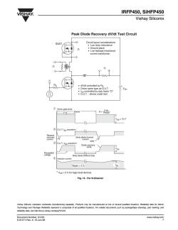
VISHAY. IRFP450,SiHFP450 Vishay Siliconix Peak Diode Recovery dV/dt Test Circuit D.U.T (+ Circuit layout considerations ·Low stray inductance ·Ground plane .Low leakage inductance current transformer 00 RG ·dV/dt controlled by RG Driver same type as D.U.T. .Isp controlled by duty factor"D" .D.U.T.-device under test ①Driver gate drive Period PW. -P.W- D=Period VGS=10 V 门】 ② D.U.T.lsp waveform Reverse recovery Body diode forward current current dl/dt ③ D.U.T.Vps waveform Body diode toard drop ④ Inductor current Ripple s5% IsD *Ves=5 Vfor logic level devices Fig.14-For N-Channel Vishay Siliconix maintains worldwide manufacturing capability.Products may be manufactured at one of several qualified locations.Reliability data for Silicon Technology and Package Reliability represent a composite of all qualified locations.For related documents such as package/tape drawings,part marking,and reliability data,see http://www.vishay.com/ppg?91233. Document Number:91233 www.vishay.com S-81271-Rev.A.16-Jun-08 1
Document Number: 91233 www.vishay.com S-81271-Rev. A, 16-Jun-08 7 IRFP450, SiHFP450 Vishay Siliconix Fig. 14 - For N-Channel Vishay Siliconix maintains worldwide manufacturing capability. Products may be manufactured at one of several qualified locations. Reliability data for Silicon Technology and Package Reliability represent a composite of all qualified locations. For related documents such as package/tape drawings, part marking, and reliability data, see http://www.vishay.com/ppg?91233. P.W. Period dI/dt Diode recovery dV/dt Ripple ≤ 5 % Body diode forward drop Re-applied voltage Reverse recovery current Body diode forward current VGS = 10 V* VDD I SD Driver gate drive D.U.T. ISD waveform D.U.T. VDS waveform Inductor current D = P.W. Period + - + + - + - - * VGS = 5 V for logic level devices Peak Diode Recovery dV/dt Test Circuit VDD • dV/dt controlled by RG • Driver same type as D.U.T. • ISD controlled by duty factor "D" • D.U.T. - device under test D.U.T Circuit layout considerations • Low stray inductance • Ground plane • Low leakage inductance current transformer RG

VISHAY. Legal Disclaimer Notice Vishay Disclaimer All product specifications and data are subject to change without notice. Vishay Intertechnology,Inc.,its affiliates,agents,and employees,and all persons acting on its or their behalf (collectively,"Vishay"),disclaim any and all liability for any errors,inaccuracies or incompleteness contained herein or in any other disclosure relating to any product. Vishay disclaims any and all liability arising out of the use or application of any product described herein or of any information provided herein to the maximum extent permitted by law.The product specifications do not expand or otherwise modify Vishay's terms and conditions of purchase,including but not limited to the warranty expressed therein,which apply to these products. No license,express or implied,by estoppel or otherwise,to any intellectual property rights is granted by this document or by any conduct of Vishay. The products shown herein are not designed for use in medical,life-saving,or life-sustaining applications unless otherwise expressly indicated.Customers using or selling Vishay products not expressly indicated for use in such applications do so entirely at their own risk and agree to fully indemnify Vishay for any damages arising or resulting from such use or sale.Please contact authorized Vishay personnel to obtain written terms and conditions regarding products designed for such applications. Product names and markings noted herein may be trademarks of their respective owners. Document Number:91000 www.vishay.com Revision:18-Jul-08 1
Document Number: 91000 www.vishay.com Revision: 18-Jul-08 1 Disclaimer Legal Disclaimer Notice Vishay All product specifications and data are subject to change without notice. Vishay Intertechnology, Inc., its affiliates, agents, and employees, and all persons acting on its or their behalf (collectively, “Vishay”), disclaim any and all liability for any errors, inaccuracies or incompleteness contained herein or in any other disclosure relating to any product. Vishay disclaims any and all liability arising out of the use or application of any product described herein or of any information provided herein to the maximum extent permitted by law. The product specifications do not expand or otherwise modify Vishay’s terms and conditions of purchase, including but not limited to the warranty expressed therein, which apply to these products. No license, express or implied, by estoppel or otherwise, to any intellectual property rights is granted by this document or by any conduct of Vishay. The products shown herein are not designed for use in medical, life-saving, or life-sustaining applications unless otherwise expressly indicated. Customers using or selling Vishay products not expressly indicated for use in such applications do so entirely at their own risk and agree to fully indemnify Vishay for any damages arising or resulting from such use or sale. Please contact authorized Vishay personnel to obtain written terms and conditions regarding products designed for such applications. Product names and markings noted herein may be trademarks of their respective owners
按次数下载不扣除下载券;
注册用户24小时内重复下载只扣除一次;
顺序:VIP每日次数-->可用次数-->下载券;
- 《电力电子技术》课程实验指导(参考资料)三相桥式整流及有源逆变电路的MATLAB仿真.pdf
- 《电力电子技术》课程实验指导(参考资料)MBR3060PT中文资料.pdf
- 《电力电子技术》课程实验指导(参考资料)E13005_NPN_晶体管.pdf
- 《电力电子技术》课程实验指导(参考资料)MAC97A6datasheet.pdf
- 《电力电子技术》课程实验指导(参考资料)BTA41-600中文资料.pdf
- 石河子大学:《电力电子技术》课程教学实验指导书(2014版).doc
- 《电力电子技术》课程实验指导(参考资料)MOS管——8N60.pdf
- 《电力电子技术》课程实验指导(参考资料)scr.pdf
- 《电力电子技术》课程实验指导(参考资料)Classification.pdf
- 《电力电子技术》课程实验指导(参考资料)IGBT.pdf
- 《电力电子技术》课程实验指导(参考资料)5SGA 30j2501.pdf
- 《电力电子技术》课程实验指导(参考资料)IGBT-INTRO.pdf
- 《电力电子技术》课程实验指导(参考资料)mosfet.pdf
- 石河子大学:《电力电子技术》课程教学资源(授课教案,任课教师:龚立娇).doc
- 西安邮电大学:《光纤传输技术》课程教学课件(PPT讲稿)第四章 有源器件技术.ppt
- 西安邮电大学:《光纤传输技术》课程教学课件(PPT讲稿)第五章 光纤传输线路技术.ppt
- 西安邮电大学:《光纤传输技术》课程教学课件(PPT讲稿)第六章 光纤信息传输系统.ppt
- 西安邮电大学:《光纤传输技术》课程教学课件(PPT讲稿)第一章 光纤技术.ppt
- 西安邮电大学:《光纤传输技术》课程教学课件(PPT讲稿)第三章 无源器件技术.ppt
- 西安邮电大学:《光纤传输技术》课程教学课件(PPT讲稿)绪论 Fiber-Optic Communication Technology.ppt
- 石河子大学:《电力电子技术》课程教学课件(PPT讲稿)第5章 直流直流变流电路.ppt
- 石河子大学:《电力电子技术》课程教学课件(PPT讲稿)第7章 PWM控制技术.ppt
- 石河子大学:《电力电子技术》课程教学课件(PPT讲稿)第10章 电力电子技术的应用.ppt
- 石河子大学:《电力电子技术》课程教学课件(PPT讲稿)第5章 直流直流变流电路.ppt
- 石河子大学:《电力电子技术》课程教学课件(PPT讲稿)第8章 软开关技术.ppt
- 石河子大学:《电力电子技术》课程教学课件(PPT讲稿)第6章 交流交流变流电路.ppt
- 石河子大学:《电力电子技术》课程教学课件(PPT讲稿)第4章 逆变电路.ppt
- 石河子大学:《电力电子技术》课程教学课件(PPT讲稿)第1章 绪论(主讲:周伟绩).ppt
- 石河子大学:《电力电子技术》课程教学课件(PPT讲稿)第2章 电力电子器件.ppt
- 石河子大学:《电力电子技术》课程教学课件(PPT讲稿)第3章 整流电路.ppt
- 石河子大学:《电力电子技术》课程教学课件(PPT讲稿)第1章 绪论(2016).ppt
- 石河子大学:《电力电子技术》课程教学资源(课件讲稿)第2章 电力电子器件(2016).pdf
- 石河子大学:《电力电子技术》课程教学资源(课件讲稿)第4章 逆变电路(2016).pdf
- 石河子大学:《电力电子技术》课程教学资源(课件讲稿)第3章 整流电路(2016).pdf
- 石河子大学:《电力电子技术》课程教学资源(课件讲稿)第5章 直流直流变流电路(2016).pdf
- 石河子大学:《电力电子技术》课程教学资源(课件讲稿)第7章 PWM控制技术(2016).pdf
- 石河子大学:《电力电子技术》课程教学资源(课件讲稿)第9章 电力电子器件应用的共性问题(2016).pdf
- 《通信原理实验》课程教学大纲 Experiments of the Communication Principle(通信工程专业).doc
- 《通信原理实验》课程教学大纲 Experiments of the Communication Principle(电子信息工程专业).doc
- 《通信原理实验》课程教学大纲 Experiments of the Communication Principle(非电类专业).doc
